The artificial intelligence semiconductor landscape stands on the precipice of a fundamental transformation, driven by an audacious engineering feat that challenges decades of conventional chip design philosophy. Cerebras Systems' wafer-scale processor represents not merely an incremental advancement in computing power, but a wholesale reimagining of how AI infrastructure can be constructed and deployed at unprecedented scale.
CEO Andrew Feldman's recent exposition of the company's revolutionary approach illuminates the profound implications of abandoning traditional chip boundaries in favor of utilizing an entire silicon wafer as a single processing unit. This wafer-scale engine fundamentally disrupts the established paradigm where individual chips are cut from wafers and packaged separately, instead creating what amounts to the world's largest AI chip spanning an entire 300-millimeter wafer surface.
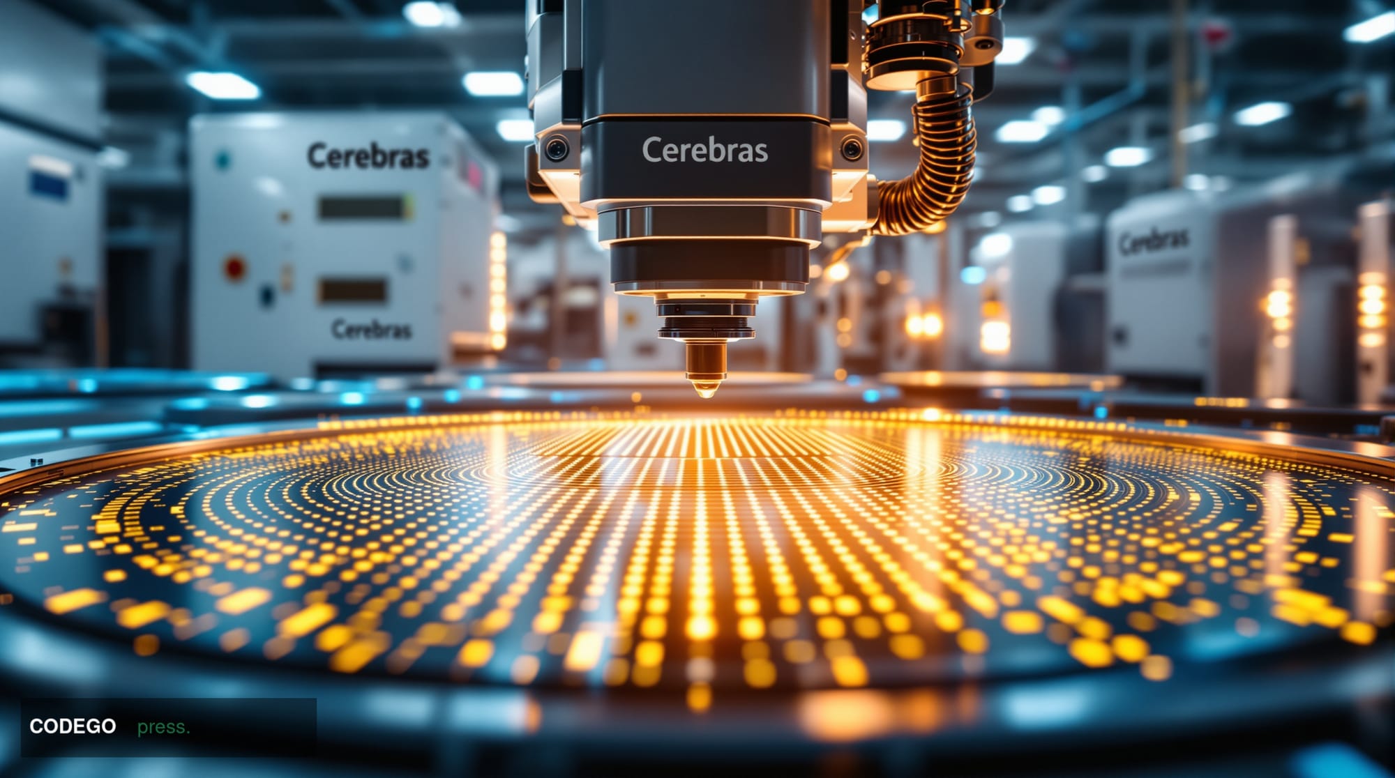
The technological audacity of this approach cannot be overstated. Where conventional AI accelerators from NVIDIA, Intel, and others are constrained by the physical limitations of individual die sizes, Cerebras has eliminated these boundaries entirely. The resulting processor contains over 2.6 trillion transistors across 850,000 AI-optimized cores, connected by a high-bandwidth fabric that enables seamless communication across the entire computational surface without the latency penalties typically associated with multi-chip configurations.
This architectural revolution addresses one of the most pressing bottlenecks in contemporary AI development: the memory wall that constrains how efficiently neural networks can access and process data. Traditional GPU clusters require complex orchestration of data movement between discrete processors, creating computational overhead that scales poorly as model complexity increases. Cerebras' wafer-scale approach places massive amounts of high-bandwidth memory directly adjacent to processing cores, dramatically reducing the time and energy required for data access patterns characteristic of large language models and computer vision applications.
The market implications extend far beyond technical specifications. As organizations grapple with the exponential computational demands of transformer-based models and multimodal AI systems, the economic calculus of AI infrastructure deployment becomes increasingly critical. Cerebras' platform promises to consolidate workloads that previously required hundreds or thousands of traditional accelerators onto a single system, potentially transforming the unit economics of AI training and inference across enterprise and research applications.
Financial institutions, in particular, stand to benefit significantly from this architectural shift. High-frequency trading algorithms, risk modeling systems, and fraud detection networks demand both massive parallel processing capability and ultra-low latency response times. The elimination of inter-chip communication delays could provide quantitative trading firms and financial services providers with measurable competitive advantages in millisecond-sensitive applications where traditional distributed computing approaches introduce unacceptable latency.
However, the path to market adoption faces substantial challenges rooted in decades of industry infrastructure optimization. Data centers worldwide have been architected around modular, replaceable components that can be incrementally upgraded and maintained. Cerebras' monolithic approach requires fundamental rethinking of cooling systems, power distribution, and failure mitigation strategies. The company must demonstrate not only performance superiority but also reliability and cost-effectiveness at scale to justify the infrastructure investments required for widespread deployment.
The broader semiconductor industry watches this development with particular interest as traditional scaling approaches face increasing physical and economic constraints. As Taiwan Semiconductor Manufacturing Company and other foundries push process geometries toward fundamental atomic limits, alternative architectural innovations like wafer-scale integration may represent the next frontier for continued performance advancement. Cerebras' success or failure will significantly influence investment patterns and research directions across the sector for years to come.
What emerges from Feldman's vision is more than a novel processor design; it represents a fundamental reconsideration of how computational resources should be organized and deployed in an era where AI workloads increasingly dominate enterprise technology priorities. The wafer-scale processor challenges not only technical conventions but also the business models and supply chain structures that have defined the semiconductor industry since its inception. Whether this approach ultimately reshapes market dynamics will depend on Cerebras' ability to translate engineering innovation into demonstrable business value across diverse AI applications and deployment scenarios.
Written by the editorial team — independent journalism powered by Codego Press.